-
10-04 08:00...大公报记者王莉杭州报道西湖大学博士后、慕德微纳(杭州)科技有限公司CEO杜凯凯说,其实最早接触到碳化硅材料的时候,并没有想到应用于AR眼镜上,“直到我们接触到透明的碳化硅之后,关注到它的折射率,才开始慢慢研究它的折射率能够带来的一些优势,然后又发现了它密度低、硬度高、热导率好等性能。”纳米级结构避免彩虹纹干扰“我们日常... 0
-
09-16 19:00...去年底投入使用的,目前已在我省的玉贤、安福两个变电站使用。”国网湖北超高压公司赵威介绍,以玉贤变电站为例,每次巡检都要检查1万多个点位,需要4个多小时,使用机械狗,不仅能节省人力成本,还有效率高,能抵抗恶劣环境等优势。与往年不同的是,今年的主会场活动更硬核,32家科研机构、企事业单位设置了展台,展示我省各行业最前沿的科... 0
-
09-13 20:10...开工就是播下希望,有海沧这片沃土滋养,我们的项目一定能茁壮成长。据悉,厦门市嘉德利新材料有限公司致力于高温型电容膜制造和工艺改进,在BOPP(双向拉伸聚丙烯薄膜)电工薄膜材料的超薄拉伸工艺和超耐温薄膜方向上取得多项突破。此次投建的项目将有助于高端电子膜材实现国产化替代,缓解国内超薄型薄膜材料供应不足的状况,形成厦门市“... 2
-
09-13 19:10...英飞凌和Schweizer与马自达共同开发出了采用芯片嵌入技术、称为“±48V系列”的新型逆变器,并在2024年6月举办的全球最大规模的功率半导体行业展会“PCIMEurope2024”上展出。虽然使用了硅(Si)功率元件,但实现了近50kW的输出功率,达到了可驱动小型纯电动汽车(EV)行驶的水平。对于英飞凌和Schw... 0
-
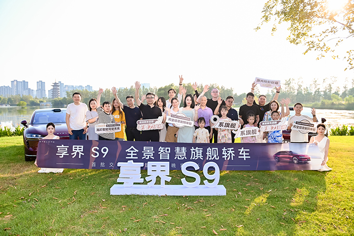
09-03 07:50...0高阶智能驾驶系统是我非常期待跟满意的,国庆我就开着它跟我老婆一起出游环游世界。“交付活动现场设置了多重互动及交流环节,如篆香体验、小岛自由行、微醺派对及乐队演出等,让所有到场的嘉宾在拥有提车喜悦同时也能与兴趣与品味相同的车主朋友共度美好时光,共同感受享界S9在豪华设计美学、极致舒适和极致智能的新体验。作为华为鸿蒙智行... 0
-
09-03 03:20...的模式建设“国家第三代半导体技术创新中心”。6中心名单中,江苏独占两席,南京和苏州成功入榜。立足创新平台优势基础,近年来,江苏在第三代半导体产业加速布局,以创新为动力、企业为主体、标志性产品为抓手,推动第三代半导体产业高质量发展。国家第三代半导体技术创新中心(南京)超净厂房里,科研人员坐在电脑前操控,一台台精密仪器自动... 0
-

-
09-03 02:20...英飞凌和Schweizer与马自达共同开发出了采用芯片嵌入技术、称为“±48V系列”的新型逆变器,并在2024年6月举办的全球最大规模的功率半导体行业展会“PCIMEurope2024”上展出。虽然使用了硅(Si)功率元件,但实现了近50kW的输出功率,达到了可驱动小型纯电动汽车(EV)行驶的水平。对于英飞凌和Schw... 0
-
08-31 21:10...“硬实力”跻身世界前列作为一家专注于碳化硅衬底材料研发、生产和销售的高科技企业,天岳先进是我国在该领域的制造业单项冠军示范企业、国家专精特新“小巨人”重点企业。2022年1月12日,天岳先进登陆A股科创板上市,是我国专注于碳化硅衬底领域首家、也是唯一的上市公司。据悉,天岳先进已实现了核心战略材料的自主可控,有力保障国内... 0
-
08-30 17:30...以及人工智能、大数据和云计算等快速发展,国内集成电路生产线增加和产能增长,存储和逻辑芯片、AI用高带宽存储器(HBI)等下游产品类别增长较快,半导体电子材料销售明显增长。研报也指出,AI大模型的快速发展对存储芯片提出了更高的要求,目前高端AI服务器GPU搭载HBM芯片已成主流,高带宽存储芯片(HBM)需求有望迎来快速增... 0
-
08-23 10:20...先后进行内科、外科、眼科、耳鼻喉科、口腔科、妇科、心理检测等10余个项目检查。同时,北京市征兵办公室还对应征女青年开展了体能测试及面试考评。应征青年李佳怡刚刚参加完第九届全国学生军事训练营的比赛,获得了优秀学生称号,这次比赛也更加坚定了她参军报国、戍守边疆的决心。作为一名预备党员,我毅然选择参军入伍,希望通过这次体检我... 0
-
08-23 10:20...包括特斯拉、比亚迪、蔚来、小鹏和吉利等。碳化硅芯片是第三代宽禁带半导体的代表性器件,是重要的新型功率半导体芯片。与传统的硅基功率半导体芯片相比,碳化硅芯片在器件效率、开关频率、工作温度等半导体器件关键性能方面明显优越,但技术仍有待完善,成本较高。中国目前发展碳化硅芯片有两大优势。一是市场需求大。中国新能源汽车发展领先,... 1
-
08-12 19:40...在中国电科旗下的山西烁科晶体有限公司,一张张小薄片,撑起公司核心科技,通过下游企业加工应用,走进生产生活。每生产一辆电动汽车,至少要消耗半片碳化硅。山西烁科晶体有限公司工作人员介绍,碳化硅有非常独特的性能优势。它具有较大的禁带宽度,使得单个器件可以承载较高的电压;较大的热导率,工作可靠性强;较高的载流子迁移率,可满足高... 1
-
-
07-16 21:00...参与探明三山岛、焦家、招平三条千吨级控矿断裂带。以六队为主建设的山东省地矿局深部找矿创新团队提出并建立了新类型黄铁矿碳酸盐脉型金矿床式,并在实践中探获威海已知最大金矿床——乳山西涝口金矿。2023年12月,由六队丁正江研究员牵头申报的“滨海地区金矿勘查评价技术与增储示范”项目获批“十四五”国家重点研发计划,在全国率先实... 1
-
07-15 10:30...发行价格为不低于定价基准日前二十个交易日公司股票交易均价的80%。对于此次募投项目的必要性,天岳先进称,碳化硅材料本身具有优异的物理性能,在下游领域应用不断深入,伴随着全球及国内在新能源汽车、新能源发电和储能等终端市场需求的快速增长,行业对碳化硅衬底需求呈现出持续旺盛的趋势。根据IHS数据,受新能源汽车行业庞大的需求驱... 0
-
07-05 17:30...将当前广受关注的二维扭转电子学研究拓展到三维体系,为调控体块材料的物性提供了新途径。相关成果以南京航空航天大学为通讯单位被《自然》刊物接收,即将正式刊发。“这是我们坚持创新驱动发展、增强自主创新能力的真实写照。”殷俊说。基于碳化硅器件的新一代新能源汽车平台充电速度提高5—10倍,续航里程提高8%以上……今年5月,中国电... 1
-
06-27 20:30...其架构和电源电路拓扑基本相似,但是它们可以根据功率级别来进行调整。以Wolfspeed参考设计CRD-60DD12N为例,这是一款采用碳化硅技术的60kW交错升压转换器,其中包含几个SiCMOSFET和二极管。在架构上采用四路交错并联,可达到60kW的调节输出功率,并同时在输出850VDC时保持99.5%的效率。该设计... 2
-
06-14 22:20...与意法半导体(中国)投资有限公司(下称“意法半导体”)将共同设立一家专门从事碳化硅外延、芯片生产的合资代工公司——三安意法半导体(重庆)有限公司(暂定名,下称“合资公司”)。合资公司预计投入总金额为32亿美元,将根据进度需要陆续投入。合资公司注册资本为6.12亿美元,湖南三安持股比例为51%,意法半导体持股比例为49%... 5
-
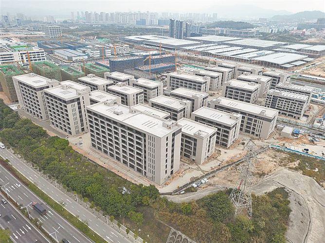
05-28 15:00...跨境电商单量突破800万单,在全省综保区综合绩效考核中排名第二。据悉,今年一季度引进落户的4个重点项目,全部聚焦汽车电子、芯片等半导体产业领域。其中,吉盛微半导体碳化硅项目投资20亿元,主要从事半导体碳化硅材料研发及生产制造,已完成公司注册、项目备案等手续,正在进行厂房装修招标,预计7月投产。京赢电子项目由深圳思赢科技... 4
-
-
05-16 23:40...有限公司董事长张清纯再次展现了该企业的强劲实力:目前该企业下一代碳化硅芯片已在多家车企进行验证,未来将率先实现主驱碳化硅芯片的国产替代。凭借更好的电子浓度和运动控制,第三代半导体材料初露头角。其制作的高温、高频及大功率电子器件,在光电子、微电子领域展现了重要价值。相比其他城市,宁波第三代半导体起步并不算早,但通过内部挖... 2
-
05-07 06:20...关于成本问题,要从碳化硅的工艺流程说起。通常情况下,高纯度的碳粉和硅粉在一定温度条件下进行反应,以生长出不同尺寸的晶锭,这一过程被称之为“长晶”,与传统单晶硅材料相比,碳化硅长晶速度十分缓慢,通常每7天才能生长2-3厘米,这是决定碳化硅材料价格较高的第一个因素。在长晶完成后,还需要通过切(切割)、磨(打磨)、抛(抛光)... 5
-
05-07 06:20...英飞凌制订了远景目标,表示将在2030年达成30%全球SiC市场份额。天科合达股东包括深创投、中科创星、国家集成电路产业投资基金、哈勃科技投资基金、比亚迪、宁德时代、润科基金等。公司成立于2006年,成立之初的主要技术源自中科院物理研究所,主要产业化支持资金来源于新疆天富集团。在导电衬底领域,天科合达在2021年国际市... 7
-
05-04 21:40...已与中国碳化硅材料供应商北京天科合达半导体股份有限公司签订一份长期供货协议,以确保获得更多有竞争力的碳化硅来源,维护整体供应链稳定。碳化硅是一种性能优异的半导体材料。相比同类硅基器件,碳化硅器件具有耐高温、耐高压、高频特性好、体积小和重量轻等优点,在电动汽车、光伏、5G等产业领域具有重要的应用价值。公报说,天科合达将为... 6
-
-


-
本页Url:
-
2024-10-05-02:25 GMT . 添加到桌面浏览更方便.
-

